What if there were a smaller computer in your computer?
It's 2020. A global pandemic rages on and the U.S. is facing one of its most difficult political divides in history. In these uncertain and anxiety-inducing times, we can only truly rely on is IEEE 1364 and Dr. Jonathan Tse. Escape to the world of register files and case statements, and embark on an intellectual journey as we walk you through our behavioral Verilog implementation of a single-cycle CPU, complete with arithmetic operations, branch and jump commands, and memory access and storage.
Goal: A Complete MIPS Processor
To implement a complete MIPS processor, we needed a complete definition of the processor’s behavior. We kept things simple by sticking to behavioral Verilog instead of structural Verilog, e.g. instead of making wires and an AND gate, we would use the AND operator to get the desired behavior.
Part 1: Base MIPS Processor
Testbench ("test_cpu.v")
The testbench for this MIPS cpu initializes the processor with compiled data/memory and a reset pulse, then provides a clock until program exit.
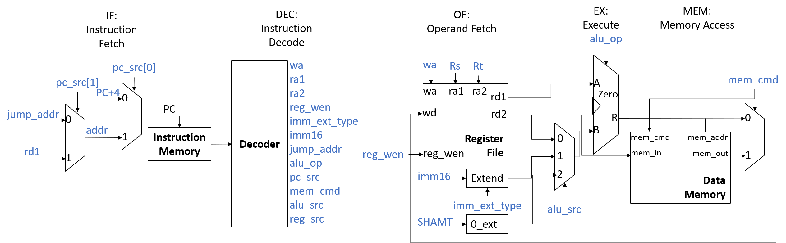
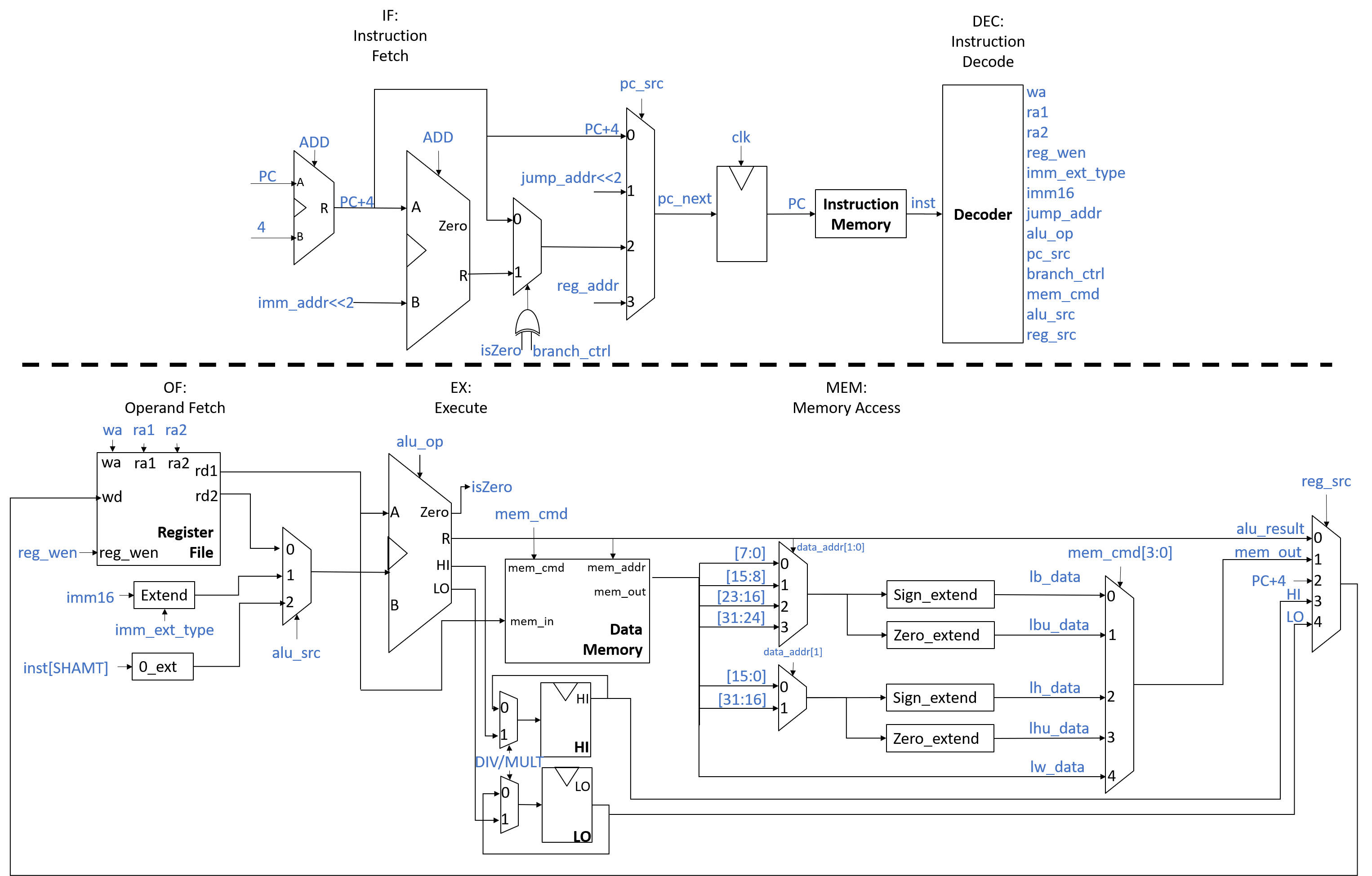
The base MIPS processor must perform the basic functions of a single-cycle CPU: instruction fetch, instruction decode, operand fetch, execute, and results store. This version of the processor implements the arithmetic logic, shifter, jump, load word, and store word instructions. In our Verilog implementation, instruction fetch logic is in module “fetch.v”; data memory and instruction memory are a single module, “memory.v”; instruction decode logic is in “decode.v”; and the arithmetic and logic of the execute step is in “alu.v”. These modules are connected to each other in “cpu.v”.
To facilitate testing, we implemented four SYSCALL functions:
- SYSCALL 1: Print the integer in register $a0.
- SYSCALL 4: Print the null-terminated string starting at address stored in register $a0.
- SYSCALL 10: Terminate execution.
- SYSCALL 17: Terminate execution with result.
Top-Level Structure (“cpu.v”)
Inputs- Clock
- Reset
- SYSCALL print outputs
The components of the MIPS processor are all declared and connected in this module. The immediate extend type, alu source, and register source multiplexers (MUXes) are here. The SYSCALL functions are executed by this module if a SYSCALL instruction is detected in the instruction independent of the decode module.
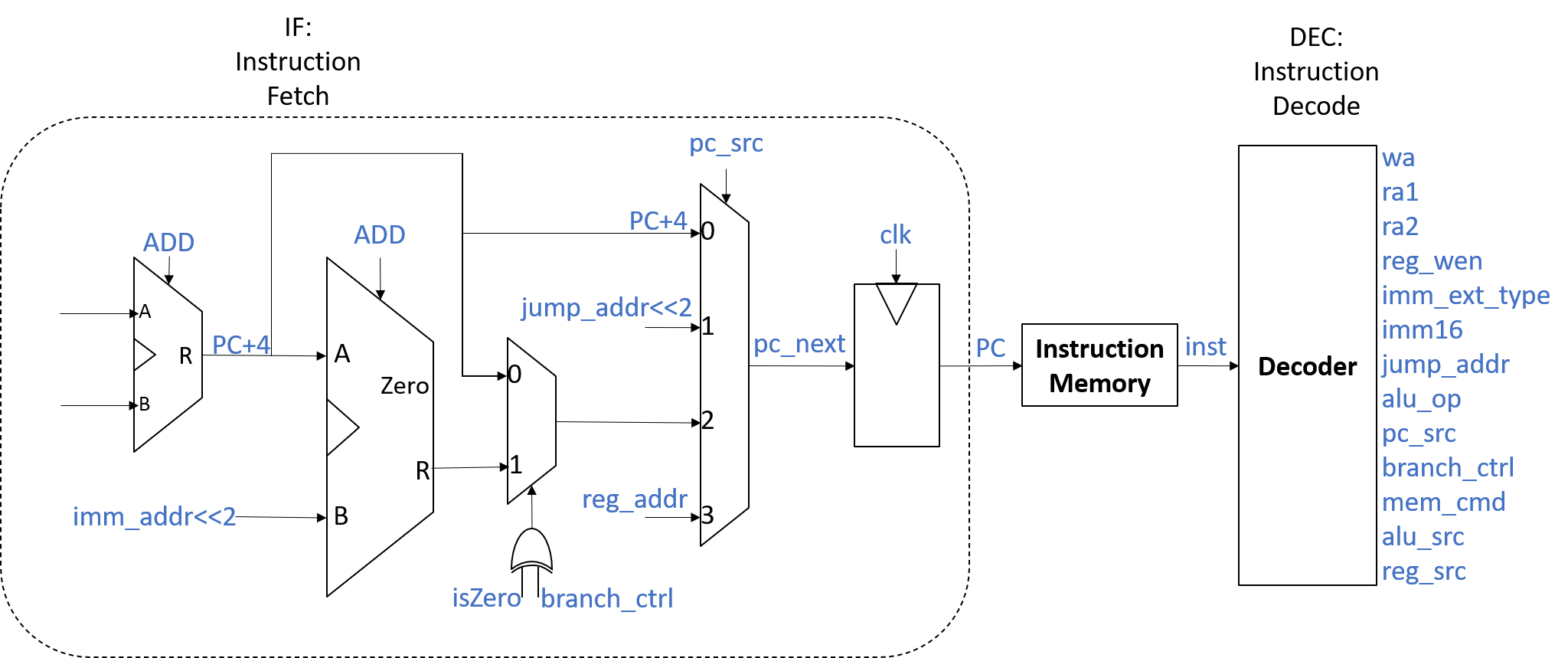
IF: Instruction Fetch (“fetch.v”)
Inputs- Clock
- Reset: If asserted, set pc_next = 0.
- pc_src: A value from 0-3 defining the source of the next value for the program counter (pc).
- isZero: A binary value which is asserted if the arithmetic logic unit has calculated a zero-valued result.
- branch_ctrl: A binary value which controls whether to perform a branch or not in conjunction with isZero, given pc_src indicates a branch instruction is underway.
- reg_addr: A 32-bit value from a register used as the complete next program counter value in jump register instructions.
- jump_addr: A 26-bit value to which the program counter is set in non-register jump instructions.
- imm_addr: A 16-bit value that functions as an offset from the current program counter in branch instructions.
- pc_next: The value of the program counter on the next instruction. Instruction is retrieved from instruction memory in the memory module.
The fetch module produces the value of the program counter according to the type of instruction and conditional information in the case of branch instructions. The program counter (pc) is word-aligned, so the lower 2 bits are always zero. If pc_src == 0 or is invalid, the program counter moves to the next instruction by adding 4. If pc_src == 1, pc_next is set to the jump address, jump_addr << 2. If pc_src == 2, pc is incremented by 4 then conditionally incremented by imm_addr if the branch condition is met. Branch behavior is described in more detail later. Finally, if pc_src == 3, pc is set to a value from the register file reg_addr.
MEM: Memory (“memory.v”)
Inputs- Clock
- Reset: If asserted, set pc_next = 0.
- PC: Program counter (instruction address).
- mem_cmd: Either a no-operation (do nothing), read, or write. The module will not read/write memory unless this is set.
- data_in: Data to write to a register.
- data_addr: The address to which to write or from which to read.
- instruction: The 32-bit instruction to be decoded.
- data_out: The value read from data_addr, if any.
The memory module has two main tasks: read the instruction from memory and perform program memory operations. The module will always produce instruction based on the value of the program counter, but memory operations only occur if mem_cmd is not a no-operation. The memory array is implemented as a 4096 element array of 32-bit words, so the lower 2 bits of the data_addr are discarded. The memory range is limited such that the upper 17 bits of both data_addr and the program counter must be zero, otherwise an error is thrown and execution stops.
DEC: Intruction Decode (“decode.v”)
Inputs- Instruction
- wa: Write register address.
- ra1: Read register address 1.
- ra2: Read register address 2.
- reg_wen: Register write enable.
- imm_ext: Type of extension (Zero or Sign) to perform on the immediate.
- imm: Immediate value.
- addr: Immediate Address for jump and branch instructions.
- alu_op: Arithmetic logic unit operation to perform, usually the function code.
- pc_src: Source for the program counter.
- mem_cmd: No-operation, read, or write memory.
- alu_src: Selects alu operand B from register data 2, immediate, or shift amount (sa).
- reg_src: Selects register write data from the alu, memory, program counter + 4, HI, or LO.
- branch_ctrl: If asserted, use invert isZero to get branch condition.
The decode module sets all the control wires according to the behavior specification in Table 2. It is implemented as a set of nested switch statements and would probably be implemented as a lookup table. Not all outputs must have a definite value for all operations.
OF: Operand Fetch (“regfile.v”)
Inputs- Clock
- Reset: Set all register values to 0, set R[$sp] = 0x3ffc.
- wren: Enable register writes.
- wa: Register address to write.
- wd: Register data to write.
- ra1: Read address 1.
- ra2: Read address 2.
- rd1: Data read from ra1.
- rd2: Data read from ra2.
The register file produces the operands for the cycle and performs any write operations if wren is asserted. Table 1 describes the registers in more detail. The stack pointer, $sp, resets to 0x3ffc and the stack grows downward.
EX: Execute (“alu.v”)
Inputs- alu_op: Which operation to perform, usually a function code from the instruction.
- A: Operand A, always rd1 from the register file module.
- B: Operand B, either rd2, zero/sign extended immediate, or shift amount.
- R: Result of alu_op on the operands.
- HI,LO: Result of multiplication and division operations.
- Overflow: Asserted if an overflow occurred, currently halts execution if asserted.
- isZero: Asserted if R == 0.
The arithmetic logic unit (ALU) takes operands as inputs and produces a result. The result is used to evaluate branch conditionals or is stored to memory/register. Signed addition and subtraction can cause overflow interrupts, in which case the processor halts.
Part 2: Branch Instructions
All branch instructions evaluate a conditional statement and branch when that conditional is met. Our arithmetic logic unit generates the isZero flag whenever the operation causes the result to be 0, and we invert this flag for certain instructions to branch if the condition is met or not. For BNE and BEQ, the arithmetic operation that causes the isZero flag to toggle on the right conditions is Subtraction. For BGEZ, BGEZAL, BGTZ, BLEZ, BLTZ, BLTZAL, the right operation is Set Less Than and a certain order for the operands. An additional flag, BranchCtrl, is asserted to invert the isZero flag via an XOR gate to generate the final doBranch flag for all “not equal” instructions (BNE, BGTZ, BLTZ, BLTZAL). BranchCtrl is not asserted for the “equal” instructions (BEQ, BGEZ, BGEZAL, BLEZ) to leave isZero as is. The decode module assigns the branch_ctrl, alu_op, and register address wires wa, ra1, ra2 to execute this behavior. For BGEZAL and BLTAL, the decode also asserts register file to write the program counter to R[$ra] via register write enable reg_wen and register file source reg_src.
| Instruction | ALU operation | branch_ctrl | isZero | doBranch (isZero XOR branch_ctrl) |
|---|---|---|---|---|
| BEQ | R[rs] - R[rt] | 0 | 0 | No |
| BEQ | R[rs] - R[rt] | 0 | 1 | Yes |
| BNE | R[rs] - R[rt] | 1 | 0 | Yes |
| BNE | R[rs] - R[rt] | 1 | 1 | No |
| BGEZ | R[rs] < R[$zero] | 0 | 0 | No |
| BGEZ | R[rs] < R[$zero] | 0 | 1 | Yes |
| BGTZ | R[$zero] < R[rs] | 1 | 0 | Yes |
| BGTZ | R[$zero] < R[rs] | 1 | 1 | No |
| BLEZ | R[$zero] < R[rs] | 0 | 0 | No |
| BLEZ | R[$zero] < R[rs] | 0 | 1 | Yes |
| BLTZ | R[rs] < R[$zero] | 1 | 0 | Yes |
| BLTZ | R[rs] < R[$zero] | 1 | 1 | No |
In “decode.v”, the decoder differentiates BGEZ, BGEZAL, BLTZ, and BLTZAL by the value in the field marked rt because they share the opcode 0x1. BEQ, BLEZ, BGTZ, and BNE are differentiated by their unique opcodes. The decoder assigns all control wires according to the behavior outlined in Table 1 and Table 2. In “alu.v”, no changes were needed since SLT, SUB, and isZero are used in their normal ways.
In “fetch.v”, all branch instructions start by incrementing the program counter by 4. If doBranch is true, indicating the branch should be followed, then add offset << 2 to the program counter. Otherwise, do nothing (regular program counter increment). Some pseudocode outlining this behavior follows:
					pc_next = pc_next + 4
					if (branch_ctrl ^ isZero)
					pc_next = pc_next + (offset << 2)
Our Verilog implementation of the above pseudocode is in part of the `PC_SRC_BRCH case in “fetch.v”.
- "branch.asm" tests BEQ and BNE by converging an initial value to a target value by half the difference each loop.
- "branchAL.asm" tests BLTAL and BGEZAL by printing four strings in order and not printing a fifth string.
- "branchEZ.asm" tests BGEZ and GLEZ by printing four strings in order and not printing a fifth string.
- "branchTZ.asm" test BGTZ and BLTZ by printing four string in order and not printing a fifth string.
While testing branch instructions, we learned that the MARS compiler, our reference for correct assembly execution, was set to use delayed branch execution. Delayed branch execution occurs in some processors and results in the instruction after any branch instruction being executed no matter if the branch is followed or not. Our Verilog processor does not behave this way, so we disabled delayed branch execution.
Part 3: Integer Multiplication/Division
Multiplication and division differ from addition and subtraction because their results are stored in two special 32-bit registers called HI and LO, as opposed to a single 32-bit output. For multiplication, the least-significant 32 bits are stored in LO and the most-significant 32 bits are stored in HI. In division, LO stores the quotient, while HI stores the remainder. There is no overflow handling needed for multiplication and division of integers. On top of implementing the HI and LO registers, we also had to implement MFHI (move from HI) and MFLO (move from LO) to retrieve the output of these operations.
"mult.asm" tests MULT, MULTU, DIV, and DIV U by utilizing MFHI and MFLO to print the output of the operations.
When we first implemented signed multiplication, or MULT, we found that the result was not producing the correct output, so we had to manually sign-extend both the multiplicand and the multiplier in Verilog to resolve the issue. We also had to explicitly mark the operands as signed for signed division, although we did not need to sign extend the operands.
The Verilog code that performs signed multiplication and division for register values A and B is not obvious, so we have included it to help the reader:
{HI,LO} = $signed({{32{A_sign}}, A} * {{32{B_sign}}, B});
LO = $signed(A) / $signed(B); HI = $signed(A) % $signed(B);
Part 4: Memory Access
We expanded the CPU's memory load and store functions by implementing load byte (LB/LBU), load halfword (LH/LHU), store byte (SB), and store halfword (SH). We first increased the width of the memory command mux control from 2 bytes to 4 to support different data sizes and sign detection. To handle the different data widths, the data addresses are conditionally sign- or zero-extended using case statements/multiplexers. The decoding of the instructions for these functions is very similar to LW and SW, but the more significant bits distinguish the data size.
"memory.asm" tests the various load and store functions by loading and storing specific values and then printing them to verify the correct values were retrieved.
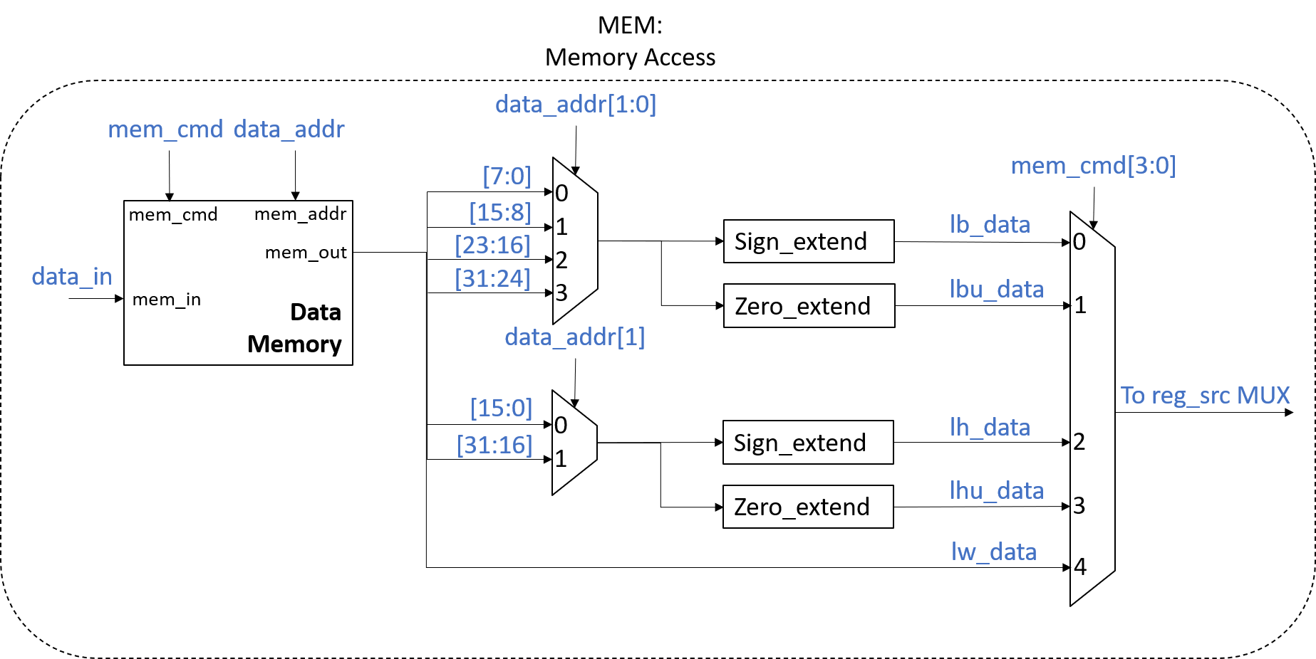
Within “memory.v”, we had to hardcode each case for the different data widths based on the last two bits of the data address. For the sake of word alignment, LB can retrieve data from any byte-aligned address, while the halfword data can only be retrieved from word-aligned memory addresses. We had to implement a similar set of case statements to store bytes and halfwords as well.
Next Steps
We have a few stretch goals that we would like to tackle in the future. These include the following features:
- Exeption/interrupt handling
- Support for floating-point arithmetic
- Run arbitrary C code on processor
- Dhrystone test